I was hoping to make this the topic of my first ever video tutorial, but I still haven't got round to cleaning my desk of all the junk and setting up a holder for my phone to use as a camera. Plus I am suffering from a bad cold right now and sound awful. So text it is.
I'd like to help you get to know exactly what a digital IO pin of an Arduino actually is and how it works. Many questions I come across along the lines of "How does this work", or "Why do you need to do this", or similar, can be answered easily if you know exactly what goes on inside an IO pin.
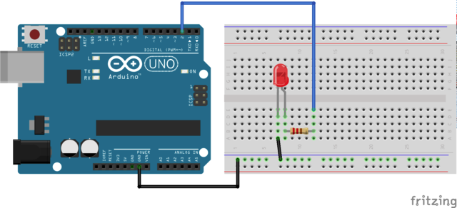
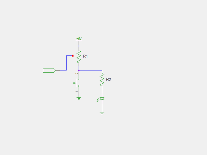
So let's start out with the first circuit that every one makes when they start with Arduino. Blinking an LED.
And the typical code:
void setup() {
    pinMode(2, OUTPUT);
}

void loop() {
    digitalWrite(2, HIGH);
    delay(1000);
    digitalWrite(2, LOW);
    delay(1000);
}
And the LED blinks.
Set the pin HIGH and it outputs 5V. Set the pin LOW and it doesn't output 5V any more. When the pin is HIGH the current flows through the resistor, through the LED, and it lights up. It's not rocket surgery.
Now, here's a fun little experiment. What happens if we turn the LED around and instead of connecting it to ground we connect it to +5V? Here's a circuit:
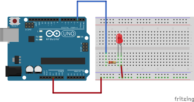
No need to make any changes to the code. Just see what happens.
You may notice that the LED still blinks. Now how does that work? The LED has to have a voltage difference across it to make it light up, surely? And if the pin is outputting 5V when it's HIGH and the LED is connected to 5V, where is the voltage difference? Well, there is one more factor there that you can't actually see: the LED is blinking backwards. Not sure what I mean? Ok, let's try this circuit - a combination of both the two above:
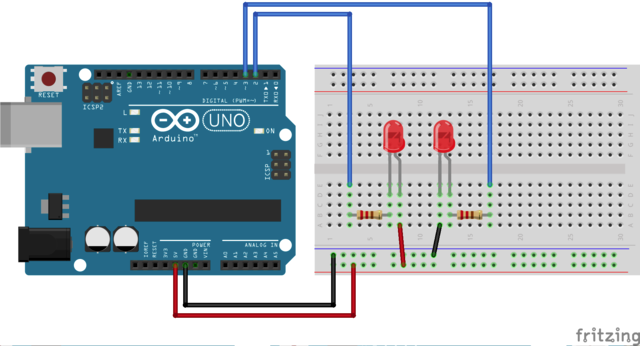
Pin 2 is connected in the traditional "LED to ground" arrangement, and pin 3 in the new "LED to 5V arrangement. And a slight change to the code:
void setup() {
    pinMode(2, OUTPUT);
    pinMode(3, OUTPUT);
}

void loop() {
    digitalWrite(2, HIGH);
    digitalWrite(3, HIGH);
    delay(1000);
    digitalWrite(2, LOW);
    digitalWrite(3, LOW);
    delay(1000);
}
Both pins are now going HIGH together and LOW together. And lo - the LEDs blink alternately!
Are you confused now?
Simply put: the LED connected to 5V is lighting up when the pin goes LOW, not HIGH. That's what I mean by it blinks backwards.
To understand exactly why you need to understand just what is inside the IO pin of the chip. So let's take a look at what an IO pin actually is. This is the block diagram from the ATMega328P datasheet. It shows is exactly what is in there:
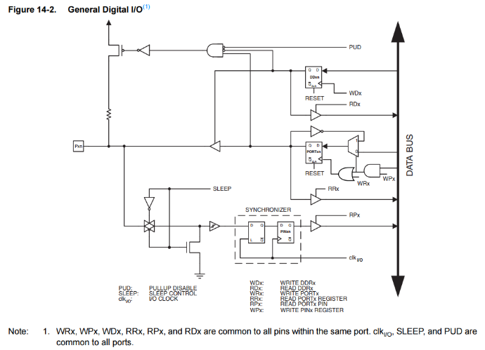
Mind boggling, yes? Actually, no. Much of it we can ignore for the moment. I'll delete all the bits that we don't currently care about so we can focus on the bits we do:
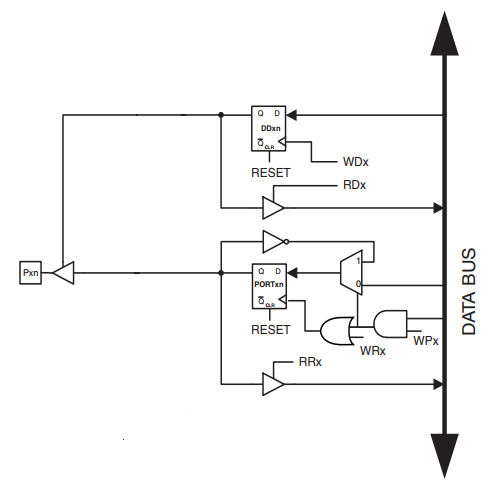
There, much simpler. So what is in there? Again, much of it we don't really care about since it represents how the internals are controlled. The three main bits we are interested in though are the two rectangular boxes DDxn and PORTxn, and the little triangle next to the pin.
The two rectangular boxes are D-type latches. Basically they store one bit of data from their input (D) and output it through their output (Q). They are how the DD and PORT registers are actually implemented. When you set the pin HIGH you are actually writing a logic HIGH into the PORTxn latch. That HIGH is then output all the time from the latch so you don't need to keep outputting HIGH all the time.
The little triangle is a buffer. It's a bit like an amplifier, and it even has a "mute" button. The latch outputs a HIGH which is 5V just as you would expect. However it's a very weak HIGH. The current it can provide is absolutely minuscule. The buffer amplifies that and allows the pin to output much more current.
The third line coming in to the top of the buffer is like the mute button on an amplifier. It allows you to turn the buffer on and off at will. And this is the key to the DDxn latch's operation, which is directly tied to the pinMode() function. When you set the pin to an OUTPUT with pinMode the latch stores that (as a HIGH). It then passes that mode on to the buffer to turn it on. When set to INPUT the latch stores that too (as a LOW) and turns the buffer off.
Simply: when in OUTPUT mode the logic value from the PORTxn latch is allowed to pass through the buffer. When in INPUT mode the logic value is blocked and can't get to the pin.
It's exactly how this buffer works that is key to understanding why the LEDs blink like they do.
So let's dig down into this buffer. The ATMega328P is a CMOS device. The simplest CMOS buffer is made up from four MOSFETS - two N-channel and two P-channel. It looks like this:
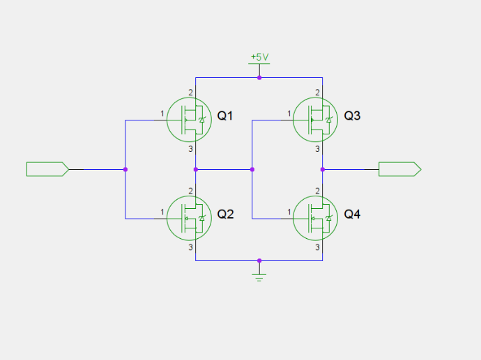
The P-channel MOSFETs are on the top (Q1 and Q3) and the N-channel on the bottom (Q2 and Q4). As you can probably see it consists of two identical stages one after the other. This is needed because of a simple problem: one stage alone inverts the signal.
The problem here is that P-channel MOSFETs turn on when their input is LOW, and N-channel turn on when the input is HIGH. You'd think that you could then just use one stage and place the N-channel on the top and the P-channel on the bottom. Unfortunately that won't work due to how the MOSFET decides what is HIGH and what is LOW. I won't go into that right now, but suffice it to say this is the best arrangement.
It's simplest to think of a MOSFET as a switch. For even more simplicity I'm going to combine both stages into one and imagine it's upside down. In effect we are going to be taking the first stage as an inverter, which we will otherwise ignore, and take the incoming signal to the second stage inverted. Confused? Don't worry, it doesn't matter.
So we'll have it so that if the input signal is a HIGH the top MOSFET is turned on. If the input signal is a LOW the bottom MOSFET is turned on.
I'm going to replace the MOSFETs with switches and add the LED and resistor so you can get a much better impression of what is happening. We'll start with outputting a LOW:
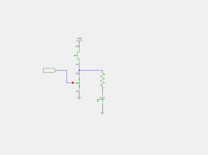
It's amazing how simple the circuit now looks. As you can see the LED can't light up because there is no connection to 5V. It's just ground, through the resistor and LED, and back to ground. It'll come as no surprise now what happens when we output a HIGH:
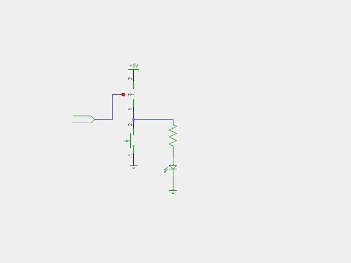
Now we have a circuit! From 5V, through the top switch (MOSFET), through the resistor and LED, and to ground! And the LED lights.
You should now be able to visualise what happens if you reverse the LED and connect it to 5V instead of ground. When we output a HIGH our circuit goes through the top switch: 5V -> switch -> resistor -> LED -> 5V. There's no connection to ground. However when we output a LOW our circuit then goes through the lower switch to ground - so we have 5V -> LED -> resistor -> switch -> ground - and the LED lights up!
It's all so simple now, isn't it? The output pin is just like a switch that either connects it to 5V or to ground.
Right, now I've made it all nice and simple for you I'm going to start getting more technical again.
The main problem with visualising the circuit as we have above is that a MOSFET isn't a perfect switch. It's more like a resistor. It has a very very high resistance when turned off, and a relatively low resistance when turned on. The off resistance is so high we can think of it as an open switch. That's fine. It's the on resistance that concerns us here. You notice I say "relatively low" not "very low" when I talk about the on resistance. That's because, compared to a switch, the on resistance is actually quite high. It's only when compared to the off resistance that it can be considered low. So I'm going to replace the top switch with a resistor and keep the output HIGH for now.
You'll also see I've named the resistors now to make it easier to refer to them.
And now we get to talk about one thing that every Arduino user has drummed into them right from the start:
You must not draw more than 40mA through an IO pin. You should not draw more than 25mA though an IO pin.
Now we have a good concept of what is actually in the IO pin we can see precisely what that statement means.
From here on in you're going to need to know Ohm's Law. I'll leave you to go brush up on it.
Right, now you know Ohm's Law we can carry on.
I'm going to also dig some values out of the datasheet:
- DC Current per I/O Pin: 40.0mA
- Output High Voltage: 4.2V
These are the two main values of interest to us. The two are bound together using Ohm's Law. You can draw, at most, 40mA through a pin (though not for a sustained period, I'll explain why in a moment). While doing that the output is guaranteed not to drop below 4.2V (for a 5V supply).
So now using our knowledge of Ohm's Law we can work out a worst-case scenario for what that resistor is.
If we have a 4.2V output that means we must have dropped 0.8V across that resistor (since 5 - 4.2 = 8). If we are drawing 40mA we can then apply Ohm's Law to it to find the resistance:
- R = V/I = 0.8 / 0.04 = 20Ω
So we are looking at that resistance being no more than 20Ω. That's actually quite high where MOSFETs are concerned, hoiwever you have to remember that this is just one MOSFET out of millions in a chip that is smaller than the tip of your little finger. So compared to a single MOSFET in a discrete package this is a really minute one. And so it can't be made any lower resistance (yet).
Now associated with Ohm's Law are a set of power calculations which tell you how much power is dissipated (heat) by a resistor. The simplest of which is P=VI - that is, the power, in Watts, is the voltage multiplied by the current. So let's do that for the internal resistance. Remember, it's the voltage dropped, which is 0.8V:
- P=VI = 0.8 * 0.04 = 0.032W
Now if you consider that the nice chunky resistor you used in your breadboard was probably one of the common 0.25W resistors, and when you consider the size of the MOSFET we are dealing with here, you can imagine that 0.032W is quite a lot of heat for such a small device. So what happens? Simple: it gets hot. And what happens when it gets too hot for too long? Simple: the MOSFET breaks.
Which is why, wile you can draw 40mA you shouldn't do it for long, since too much heat builds up and the MOSFET will break. The recommended maximum is 25mA. So let's calculate the power that 25mA would dissipate with the same worst-case resistance of 20Ω:
- P=I²R = 0.025² * 20 = 0.000625 * 20 = 0.0125W
As you can see a reduction of less than half the current has resulted in a reduction of much more than half of the power dissipation.
Much less heat generated.
And now we come on to another linked question that I often find:
But why must I use a resistor with an LED on my Arduino? If I don't use one it still works.
I hope now that you have got this far you have learned enough to immediately know the answer to that.
So an LED connected directly to an IO port. You can see now that there is a resistor in there, which is why it still works. However, it works for now...
A 5V supply, with a 20Ω (worst case from above) and a typical red LED with a 2V forward voltage. Across the resistor, because there is 2V across the LED, 3V will have to be dropped. That means (since I=V/R) 3/20 = 0.15A (150mA) must be flowing through the resistor and the LED.
Not only are you way above the 40mA absolute maximum of the IO pin, but you're way above the (typically) 30mA absolute maximum of the LED. It's not going to survive. Something's gotta give.
And at 0.45W (I'll let you work out how to get that number - hint: the calculation is just up the page) the MOSFET in the IO pin is most likely to be the weakest link in the chain.
And now you know all about how a GPIO pin works in OUTPUT mode. I'm hoping to do more of these detailing the other modes of operation.