I thought I would take a look inside a power supply that I suspected was a counterfeit. See just what is going on with it. This Samsung power supply was making strange things happen with my phone while it was plugged in. Yes, it charged the phone fine, but it made the touch screen go all screwy, and I suspected it was a rather noisy switcher in it. I had bought it from eBay for next to nothing, so I am expecting it to be somewhat nasty inside.
Guess what? I was right.
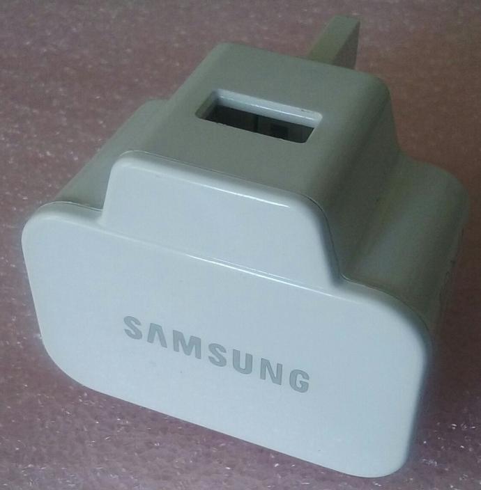
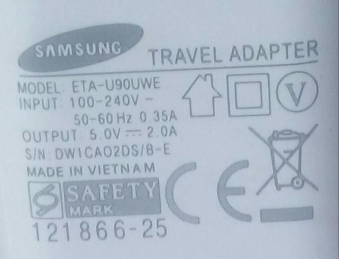
The panel on the side of it all looks very posh and legitimate. Nice crisp printing, no smudges, blurring, etc. From the outside it's almost impossible to tell that it's counterfeit. But just wait until you see inside. Do I have a treat in store for you...
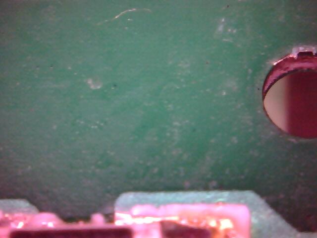
Here's what I found when I prised the lid off:
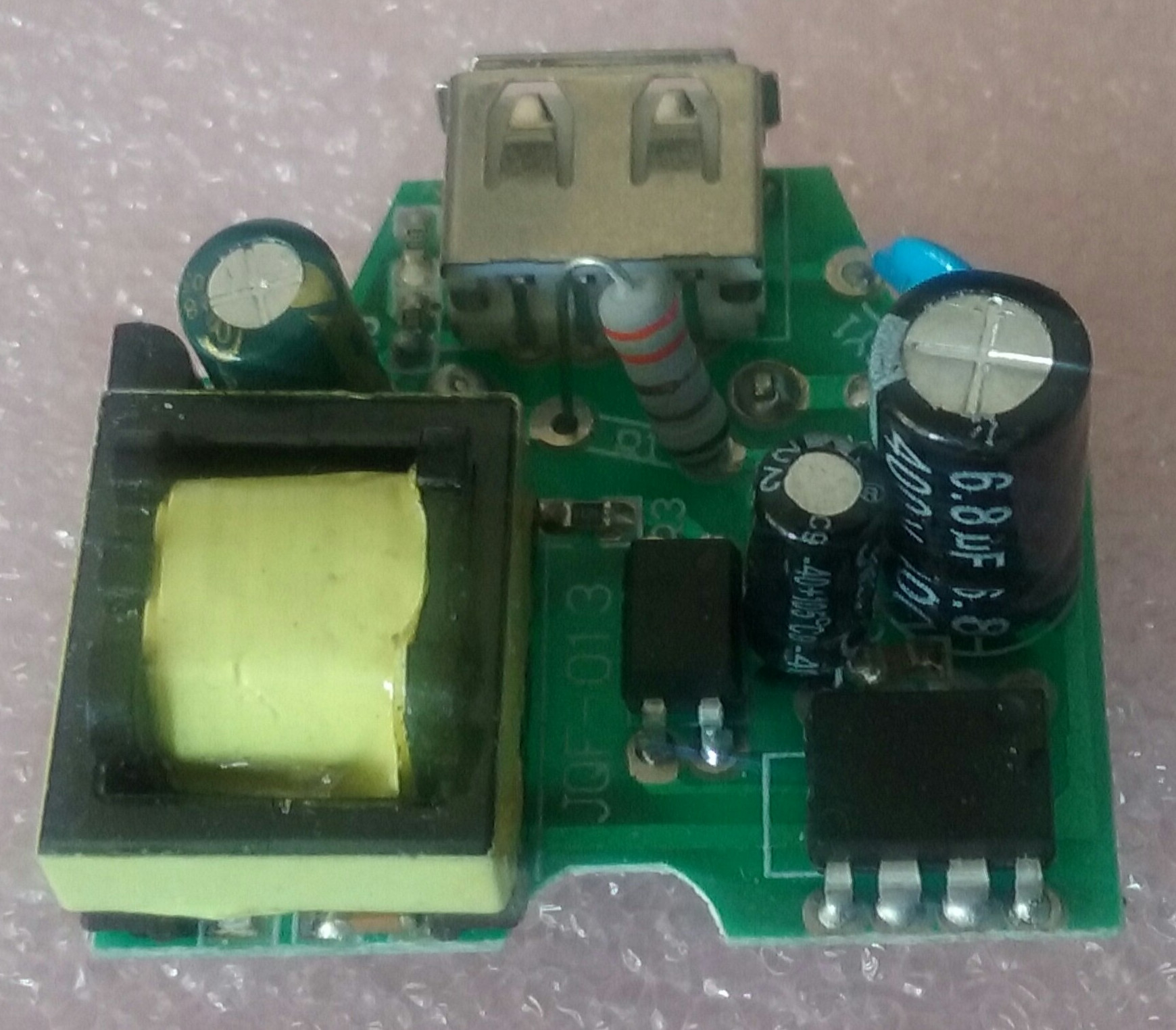
Right off the bat I can see a number of things that really make me want to scream. Things that are not just foolish, but down-right deadly.
Case the first: Mixing high and low voltage.
There are rules and regulations about mixing high voltage circuits and low voltage circuits, including clearances, isolation, insulation, etc. Rules that are supposed to stop this kind of thing happening:
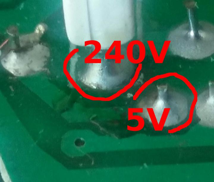
Yes, that really is the mains input pin there, and yes that really is the +5V pin of the USB connector right next to it. And that's not all. There's worse on the other side:
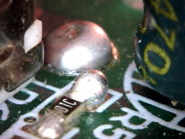
The big dome at the top is the (rather shoddy) soldering for the other mains power pin (240V) and a hair's breadth away from it a very poorly soldered resistor connecting to the data pins of the USB. That big blob of solder on the far end of the resistor is a fraction of a millimetre away from the mains. Very very nearly within arcing distance. And of course the metal on the left of the image is the shielding on the USB socket...!
All right, I'm scared now. This is getting silly.
There's more poor soldering around as well though. Some leads have barely enough solder to hold them in place. No wicking through the holes has occurred:
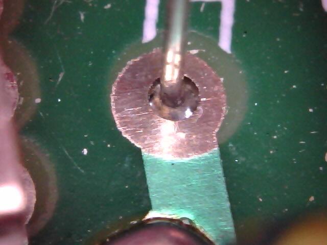
And yes, that is mains in that part of the circuit.
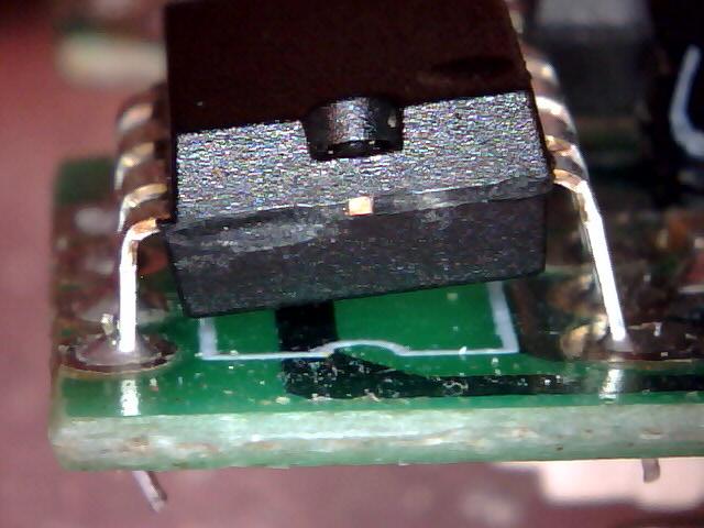
Mind you it doesn't bode well when they can't even solder a chip in straight:
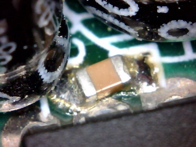
That might, though, be because of the extra capacitor bodged into the circuit as an afterthought:
If I were Samsung and that kind of quality was being created in my factories I would be screaming blue murder and people would be losing their jobs very rapidly. And so there is only one conclusion:
IT IS 120% COUNTERFEIT.
Not to mention incredibly deadly.
So let's see what is actually on this board then. Well, the main DIP chip has no markings. No, they haven't been scrubbed off - this chip never had any markings. Ever. That should ring alarm bells for a start. However there is one other device that can shed some light on this circuit - the TO-92 device to one side.
That is a DK450 - a cheap chinese voltage controller (like a voltage regulator) which is what monitors the output 5V power and tells the main switching circuit what to do. It's quite clever in some respects, since it keeps component cost down, but is not a good component in other respects. Here's a little circuit snippet from the datasheet:
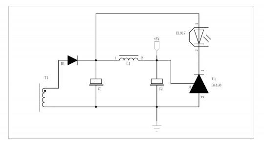
And here is another snippet found online as an image:
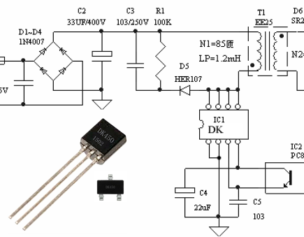
So I can see the mains portion of the circuit, the lower picture, looks to be pretty much the same as I have in front of me - with a couple of minor differences. Removing the transformer reveals C3, R1 and D5 in that schematic:
It also revels the fact that one of the pins of the transformer (the one that connects to ground in the upper schematic) has no annulus on the upper side of the PCB at all. Bit silly that really.
So we are looking at pretty much the same schematic there. The minor differences are the addition of a MOV just after the bridge rectifier (which is a nice addition actually), and for some reason the inclusion of a 3.3Ω resistor (the big grey one) in the mains input feed to the rectifier. Current consensus seems to be that the resistor is being used as a "fuse". If there is a short too much current will flow (up to about 100A) which will turn the fuse into a ~50KW furnace. That not only destroys the fuse, but the power supply, and everything around it. One way of hiding the evidence I guess...
The output side of the circuit though does have more differences - and these are the important ones.
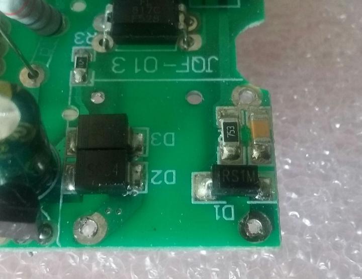
As far as I can make out, D1 in the upper schematic is D2 and D3 in the image just above - two diodes in parallel. I guess that must be because it worked out cheaper to do that than to have a single diode that was rated at the proper current. Then we have one single 470µF capacitor for C1 in the upper circuit. Also there is the addition of a small 0603 resistor on the R (side) pin of the DK450, which again looks like it's been jammed in as an afterthought:
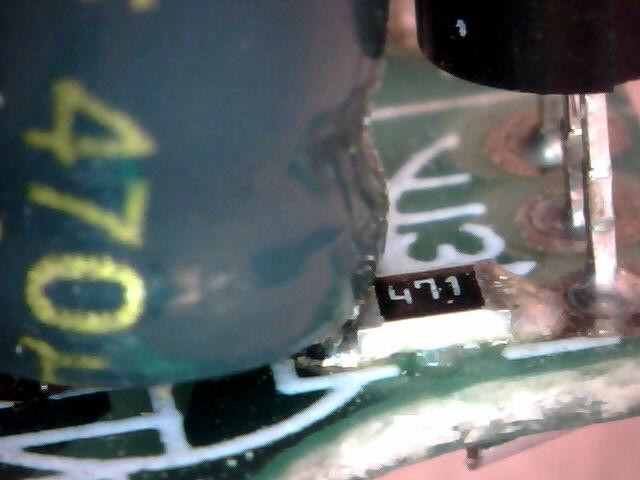
Yes, that really is underneath the capacitor.
So where is the inductor? Where is the second output capacitor? Where, in short, is the Pi filter on the output? Well, it's right here:
That's right. It doesn't exist. They didn't bother with it. And that is, as you can imagine, why the charger makes the phone go all screwy. Not only is it somewhat noisy - they have made absolutely no attempt whatsoever to create a stable voltage out from the transformer.
It is, basically, a half-wave rectified signal with a single smoothing capacitor and a bit of feedback from that noisy signal.
So the DK450 can't do its job right, since the voltage it is monitoring isn't stable, and that causes the whole switching to be wrong, creating the wrong voltage on the output, which the DK450 can't fix because it's too noisy. So maybe they added that extra 470Ω resistor on the R pin to try and offset it slightly so that it got closer to 5V? Who knows.
So to summarise:
- This power supply is DEADLY.
- The circuit is an inferior design
- It is lacking important parts of the required circuit
- The output will be horrendously noisy
- Do not buy one of these if you value your continued existence or the continued existence of your mobile device.